
Carat has extended integrated, in-situ Bias-Enhanced Nucleation to 100 mm silicon wafers. For diamond-on-silicon programs, BEN gives customers a route to nucleation that is continuous with growth, contamination-controlled, and free from mechanical slurry abrasion. The goal is better adhesion, fewer interface voids and particles, and lower thermal boundary resistance than comparable seeded interfaces.
Send substrate dimensions, target diamond thickness, required surface finish, application environment, and any acceptance criteria. Carat can help determine whether the proper next step is a sample coating, process development program, material supply discussion, or reactor configuration review.
Representative Raman spectroscopy at 532 nm on a 115 micron thick diamond layer shows a strong diamond peak centered near 1332 cm-1 with no graphitic shoulder. Across seven points along the 100 mm wafer diameter, the reported average FWHM was 3.8 cm-1 with a 0.8 cm-1 standard deviation.
This supports the central technical claim: Carat's high-power MWCVD platform can produce high quality, wafer-scale CVD diamond films suitable for thermal, photonic, detector, and advanced device development.
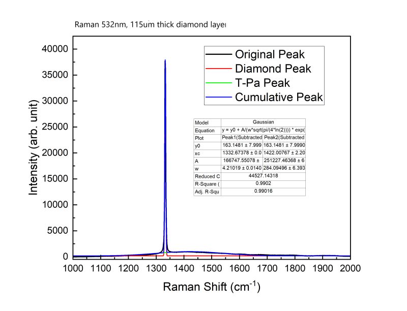
Representative Raman spectrum at 532 nm for a 115 micron thick CVD diamond layer. The diamond peak is centered near 1332 cm-1.